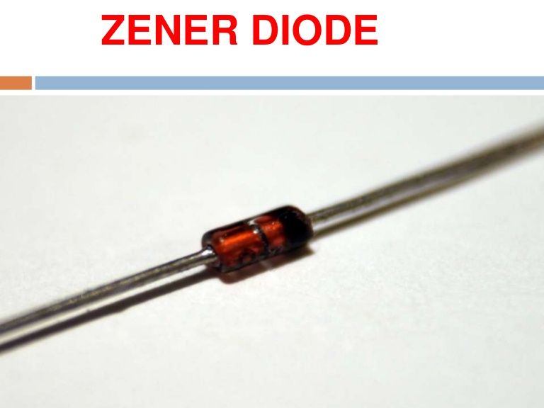
Zener diode is a special type of P-N junction diode. It is a silicon semiconductor device in which both P and N junctions are heavily doped due to which it forms a very thin depletion layer which results in the high electric field across the junction. It can work in both forward bias and backward bias, i.e., it can allow the current to flow in both forward or backward directions if enough voltage is passed across the junction, but it is mainly designed to work in the reverse direction. Zener diode solves a vast number of problems that may occur in circuit designing. Hence, it is a widely used component in electrical circuits. It is designed in such a way that it can handle the breakdown caused by the reverse breakdown voltage without failure, which is why it is also known as the breakdown diode.
Clarence Melvin Zener (1905-1993)

Zener diode is named after Clarence Melvin Zener, an American physicist, who elaborated the electrical properties of the Zener diode. He was a physics professor at Carnegie Mellon University, and his main area of interest was ‘solid-state physics.’ He did his graduation and doctorate from the Stanford University, California. In 1934, he published a paper that explained the breakdown of electrical insulators, and in the year 1950, he developed the Zener diode and started its application in computer circuits.
Construction of Zener Diode
Zener diodes are manufactured using various methods. The most widely used manufacturing methods include alloy diffused structure, passivated structure, and diffused structure. In the diffused structure, both P and N substrates are diffused together, and a metallic layer is deposited on both sides that connect the anode and cathode terminals. In an alloy diffused structure, all the junction is covered with a layer of silica oxide (SiO2), but in passivated structure, only the edges of the junctions are coated with the silica oxide layer. The Zener breakdown voltage of the diode is fixed at the time of its manufacturing, and it usually lies between 2.4V to 200V. The functioning of the Zener diode depends upon its doping level. The lightly doped diodes show avalanche breakdown, while the heavily doped diode shows Zener breakdown. Alloy-diffused Zener diodes work better at low Zener voltages while diffused and passivated structures work better at high Zener voltages.

Circuit Symbol of Zener Diode
The circuit symbol of the Zener diode is almost similar to the normal diode circuit symbols with a slight difference that the vertical line of the Zener diode symbol is slightly bent inward and outward from the upper and the lower end respectively.

Symbol of Zener Diode
Circuit Diagram of Zener Diode
Zener diode can be connected in both forward biased and reverse biased, but it works as a normal diode in forward biased condition, and it is mainly designed to work in the reverse biasing condition. In reverse biased condition, the P-type, i.e., the positive side of the diode, is connected to the negative terminal of the battery, while the N-type, i.e., the negative side of the diode, is connected to the positive terminal of the battery.

Understanding Zener Diode
The Zener diode is a heavily doped P-N junction diode; due to heavy doping, the depletion region between the P-N junction becomes narrow, and the intensity of the electric field increases. Hence, the conductivity of the Zener diode also increases. There isn’t any flow of current through the diode if no biasing is applied across the Zener diode as there will be no flow of electrons from the valence band of the P-type region to the conduction band of the N-type region. If the reverse biasing is applied across the Zener diode, and the voltage supplied exceeds the Zener voltage, then the electric field across the junction increases and the valence electrons gain enough energy and start moving from the valence band of the P-type region to the conduction band of the N-type region, and the barrier between the P and N region reduces. At the Zener voltage, the depletion region vanishes completely, and the Zener diode starts conducting.

Working of Zener Diode
In forward-biased conditions, the Zener diode works as a normal diode, but when it is operated in the reverse-biased, the depletion layer between the junction gets narrow, and it continued to become narrower if we increase the reverse-biased voltage. Initially, the current flowing through the circuit is due to minority charge carriers, but after a certain value of reverse voltage, breakdown occurs. Zener diode has two types of breakdowns, i.e., Avalanche Breakdown and Zener breakdown, which are discussed below.
Avalanche Breakdown
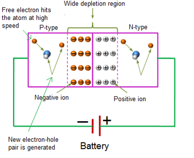
Avalanche Breakdown usually occurs if we apply very high reverse bias voltage. In the reverse biased condition, current flows through the circuit due to minority charge carriers. If we apply high reverse voltage, then these minority charge carriers get accelerated and gain high velocity, hence their movement increases. Due to their rapid movement, they collide with their surrounding atoms and generate more free electrons, and these free electrons also cause collisions that result in the generation of even more free electrons, hence a high current flows through the circuit due to the increase in the number of charge carriers. This phenomenon is known as the Avalanche breakdown. Normal diodes usually get destroyed due to this breakdown because of the generation of heat due to a high amount of current and high voltage drop, but the Zener diode is designed in such a way that it does not get damaged due to the Avalanche breakdown and can withstand the high current flow. Avalanche Breakdown is usually observed in those Zener diodes which have a Zener diode voltage of more than 5 volts.
Avalanche Breakdown Mechanism
Zener Breakdown
Zener breakdown phenomenon is commonly observed in the heavily doped diodes. Because of the high doping concentration, the depletion layer is of very narrow width. If we increase the reverse potential, it results in the generation of a strong electric field in the depletion region. Due to this high electric field, the electrons (Depletion region electrons) gain high energy and detach themselves from their parent atoms, and a large number of free electrons are generated due to this action. The movement of these free electrons causes the flow of electric current through the diode. An immediate increase in the electric current is thus observed on increasing the reverse voltage by a small value. The current increases to a maximum value, and then it stabilizes and remains constant for different values of applied voltage. When the electric current increases beyond the capacity of the diode, then the breakdown occurs, and this breakdown is known as Zener breakdown, and the voltage at which it occurs is known as Zener voltage. Zener Breakdown can be controlled because the number of valence electrons generated can be controlled by controlling the electric field in the depletion region. Commonly used Zener diodes show the Zener breakdown below 5 volts, and they have a negative temperature coefficient, i.e., if the temperature of the junction increases, Zener breakdown voltage decreases.

Differences in Avalanche Breakdown & Zener Breakdown
- Avalanche breakdown occurs due to the collisions between the electrons in the depletion region, while Zener breakdown occurs due to the strong electric field.
- Avalanche breakdown occurs in the lightly doped P-N junction diodes, but Zener diode occurs in the heavily doped P-N junction diodes.
- The diode can not attain its initial position after the avalanche breakdown, but it can regain its initial position after the Zener breakdown.
- There is a higher electric field in the depletion region in the case of Zener breakdown than the avalanche breakdown.
- In the case of avalanche breakdown, both the pairs of holes and electrons are produced, but Zener breakdown is caused only by the flow of electrons due to a high electric field.
- The avalanche breakdown occurs due to high reverse voltage, whereas Zener breakdown occurs due to low reverse voltage.
- Avalanche breakdown has a positive temperature coefficient, i.e, it increases with the increase in the temperature, while Zener breakdown has a negative temperature coefficient, i.e., it decreases with the increase in the temperature.
- Zener breakdown shows a sharp curve in their V-I characteristics as compared to the avalanche breakdown.
V-I Characteristics of Zener Diode
V-I characteristic or Volt-Ampere characteristics is a graph that represents the change in current with respect to the change in the voltage applied across the junction. The V-I characteristics of the Zener diode are divided into two categories, i.e., Forward characteristics and Reverse Characteristics. Let’s discuss them in detail.

Forward Characteristics
The forward-biased characteristics of the Zener diode are represented in the first quadrant of the graph shown above. It is clearly observed from the graph that the forward-biased characteristics of the Zener diode are the same as the normal P-N junction diode, i.e., if we increase the voltage around the terminal, then the current flowing throw the circuit also increases. However, the amount of current flowing through the Zener diode is higher as compared to the normal P-N diode due to the higher doping concentration in the Zener diode.
Reverse Characteristics
When the Zener diode is operated in the Reverse-biased condition, then initially, only a small amount of leakage current flows through the circuit due to minority charge carriers that are thermally generated, but when the applied reverse voltage is increased further to a certain value of reverse voltage, then the breakdown occurs, and a sharp increase in the reverse current is observed. The value of the reverse voltage where the breakdown has occurred is known as the Zener voltage (Vz), and this breakdown effect is known as the Zener Effect. By using external resistance, the current passing through the Zener diode can be limited. The voltage (V) through the diode can be calculated mathematically using the following expression,
V=Vz+IzRz
Where Vz is the Zenere breakdown voltage, Iz is the Current flowing through the Zener diode, and Rz is the Zener resistance.
Specifications of Zener Diode
While manufacturing a Zener diode, various types of specifications are carefully considered. Each specification impacts the overall functioning of the Zener diode. By observing these specifications we can understand the performance ability of any specific Zener diode. Here are some specifications of the Zener diode.
1. Zener Voltage (Vz)
Zener voltage is the voltage across the Zener diode at which the breakdown occurs so it’s also known as the reverse breakdown voltage. While manufacturing Zener diode their breakdown voltage is usually kept between the range 2.4 V to 200V. However, for the surface-mounted devices, the maximum Zener voltage is around 47 volts.
2. Maximum Current (Iz-max)
Iz-max is the maximum current that can flow through the Zener diode at the reverse breakdown voltage. It ranges from 200μA to 200A. Iz-max can be calculated using the formula,
Iz=Pz/Vz
Where Pz is the maximum power that the diode can handle, and Vz is the reverse breakdown voltage.
3. Minimum Current (Iz-min)
Iz-min is the minimum amount of current that is required to cause the breakdown in the Zener diode. It ranges from 5mA to 10mA.
4. Power Rating (Pz)
Power rating is the maximum power that a Zener diode can dissipate safely. Commonly used power ratings for the Zener diode include 400 mW, 500mW, 1mW, 3mW, and 5mW. Zener diodes with high power ratings are usually costly, and they require additional devices for the removal of excess heat. Maximum power dissipation (Pzm) by the Zener diode can be calculated by the given formula,
Pzm= Iz*Vz
Where Iz is the maximum current that can flow through the Zener diode, and Vz is the Zener breakdown voltage.
5. Zener Resistance
Zener resistance or Zener impedance is the total resistance offered by the Zener diode to the flow of electrical current. The Zener resistance is also evident from the reverse V-I characteristics graph as it is not completely vertical, hence there is a slight change in the current flow for the small change in voltage across the Zener diode, and this change in the voltage with respect to the current is the resistance offered by the Zener diode. Ideally, it should be zero, but every Zener diode offers some amount of Zener resistance.
Zener impedance of a Zener diode is calculated by the formula,
R=Vi-Vz/Iz
Where Vi is the input voltage, Iz is the current passing through the Zener diode, and Vz is the Zener breakdown voltage.
6. Zener Diode Tolerance
Tolerance of the Zener diode is defined as the range of voltages near the breakdown voltage at which the Zener diode conducts the current in reverse biasing. While manufacturing the Zener diode, slight differences in the doping concentrations for the same type of Zener diode may occur, which means their breakdown voltages also vary slightly, hence the same type of Zener diode conducts reverse current at different values of reverse breakdown voltage, and this range of Zener breakdown voltage is called their tolerance. Usually, the voltage tolerance for the Zener diode is ±5%.
7. Temperature Stability
The reverse breakdown voltages of the Zener diodes vary with the different temperature conditions, and it shows a large difference in its value for different degrees of temperature ranging from 0°C to 50°C. So, temperature stability is an important criterion that needs to be noticed while using Zener diode in different electrical circuits. As we read above that the avalanche breakdown has a positive temperature coefficient, and it dominates above 5 volts, while the Zener breakdown has a negative temperature coefficient, and it dominates below 5 volts. Keeping this in mind, the Zener diodes of 5 volts breakdown voltage are manufactured usually as they provide better temperature stability.
8. Junction Temperature
As the reverse electric current passes through the junction of the Zener diode, heat is generated there, so the junction area is comparatively hotter than the outside case of the Zener diode because heat is dissipated from there. While manufacturing a Zener diode, proper specifications of the internal temperature and external temperature of the diode should be employed carefully. Typically, the Zener diode junction temperature is kept between 175°C to 200°C.
9. Package
Zener diode is packaged in many different ways. However, the widely used packaging methods include traditional leaded devices and Surface mount packaging (In Surface Mount Technology (SMT), various electrical components of the device are mounted directly on Printed Circuit Boards (PCB) surface). The packaging is chosen according to the requirement of the heat dissipation level in the device.
Applications of Zener Diode
Voltage Regulator
One of the most important Zener diode applications is that it is used as a voltage regulator. The function of a voltage regulator device is to maintain the constant output voltage for a wide range of input voltages and currents. For using the Zener diode as a voltage regulator, a shunt resistance (Rs) is connected in series with the input voltage and Zener diode. Further, the load resistance is connected in parallel with the Zener diode in reverse bias mode. The Shunt Resistance Rs cut off the excess amount of current, and it allows only the limited current to pass through the Zener diode, and hence controls the voltage fluctuations and maintains the constant output voltage across the load resistance {R}_{L}.

Over-Voltage Protection
Sometimes the current in the electrical devices exceeds the normal value that can damage the device, but this damage can be minimized by using Zener diode in the electrical circuit as it protects the circuit by regulating the input voltage, and it allows the constant voltage at the output terminal. Zener diodes, along with Silicon control Rectifier (SCR), are used in various circuits as they control the high power and high voltages in the electronic circuits.

Electrical Switches
Zener diode has the ability to produce sudden changes from minimum current to maximum current, which is why it can be used as a switch.

Multimeter Protection
Another important application of the Zener diode is that it is used to protect the multimeter. Zener diode is connected in parallel with the multimeter, and it regulates the voltages and protects the multimeter from getting damaged by the excess amount of current flow in the electrical circuit. Zener diode can easily withstand high breakdown voltages as they have high doping concentration in them.
Waveshaper or Waveform Clipper
Zener diode is also used as a wave-shaper as it can modify the AC waveform and can convert the sine wave into a square wave. To achieve this, two Zener diodes facing each other are placed in series with the resistance R. The Zener diode offers high resistance if the input terminal voltage is less than the Zener breakdown voltage during the positive and negative half cycle of the input sine waveform, and the voltage across the Zener diode (Vz) will appear at the output terminal (Vo). The Zener diode offers low resistance if the input voltage is more than the Zener breakdown voltage, which allows the large current to pass through the Zener diode, and we see a large voltage drop across the resistance R and Zener diode clip-off the excess voltage, hence the input sine waveform gets clipped off. In this way, we can obtain a square waveform at the output terminal. Thus, the Zener diode is used as a wave clipper, and these circuits are mostly used in removing the interference in TV and FM transmitters.

Voltage Shifter
Zener diode can act as a voltage shifter. If we use Zener diode and resistance R in the circuit, the input voltage can be shifted to the Zener breakdown voltage.

Zener Diode Advantages
- Zener diode is cost-effective.
- It maintains and regulates the input voltage.
- It has a simple circuit and is very compatible.
- It is widely used in electrical circuits to protect devices from overvoltages.
- It provides a constant voltage at the output terminal.
- It has the ability to control the excess flow of current in the circuit.
- It is used as a waveform clipper.
Zener Diode Disadvantages
- To cancel out the excess input voltage, the Zener diode applies even more reverse voltage that consumes a lot of electricity in this process.
- Zener diode is not suitable if the load current is very high as their efficiency reduces at high load currents.
- Due to Zener resistance, the output voltage changes slightly.
- It shows high internal impedance in the circuit.
- Transistors are more preferred over the Zener diodes for regulating voltages as they have a better regulation ratio.
- As the Zener voltage equals the output voltage (Vo=Vz), we can not adjust the output voltage.